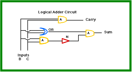
In the 19th century George Boole invented Boolean algebra as a theoretical study. In the 20th century, Boolean algebra has become the basis for designing circuits to manipulate binary numbers. Because the 0,1 of binary numbers can be represented by true (1) and false (0), circuits can be analyzed by Boolean algebra. This is very important because the analysis of a circuit can be independent of how it is realized by a specific technology. Currently, the prevalent integrated circuit technology is electric circuits embedded in 1/4" squares of silicon known as chips. (Digression on vocabulary: In your readings you will find some writers use the term chip for the integrated circuit, not just the 1/4" square of silicon on which the circuit is embedded.) Someday the technology could switch to laser light in light circuits. The presently designed Boolean circuits could be realized in the new technology without necessitating a redesign. To gain an idea of how Boolean algebra might be employed, let us consider how we might add two numbers, B and C, where each number can take on values of 0 or 1. It turns out that all arithmetic operations can be performed using three Boolean operators, which are "and","or", and " not".
| Operator |
Definition |
|---|---|
| __B__ |
__C__ |
_Sum_ |
Carry |
|---|---|---|---|

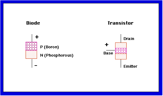
There are numerous physical ways that circuits with the 0,1 property of binary numbers can be constructed: a magnet has a north and a south pole, a switch is either open or closed. The circuits could use electricity, fluids, light, or possibly even biological circuits at the atomic level. The current primary technology is electronic and employs a device called a transistor. To understand what a transistor is, you must first understand what a diode is. A diode is a device which transmits a current only one way. While there are many ways of constructing diodes, let us consider the silicon semiconductor technology. Consider the diagram below. One block of silicon is doped with boron and the other with phosphorus. The silicon atoms are bonded together in a lattice with 8 electrons in the outer shell. Doping with phosphorus replaces some of the silicon atoms with phosphorus atoms which means there is a free electron. Doping with boron leaves the lattice one electron short creating a plus charge. Only one combination of plus and minus voltage will produce a current across the diode. If the + is attached to the p (boron) end and the - to the n (phosphorus) end, the + repels the positive charges and the - repels the electrons resulting in an electron flow across the device. In the opposite case the charges in each half are attracted to the terminal and no current flows. Thus the diode possesses an asymmetric property which provides a basis for manipulating binary numbers. A transistor, which consists of two diodes placed end to end, provides an asymmetric device which amplifies the input signal. A positive voltage at the base allows current to flow from the emitter to the collector. A negative voltage at the base causes no current flow. The transistor pictured is a pnp transistor. There is also a npn transistor which is activated by a drop in voltage.

Click here for a more complete explanation of a transistor.
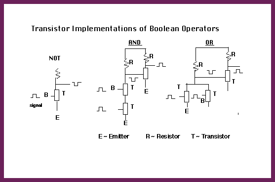
Construction of the "and", "or", and "not" using transistors. The following circuits define the "and", "or", and "not".

a. At first circuits were made with individual components wired together.
b. Later, individual components were soldered into circuit boards.
c. The creation of an integrated circuit( frequently called a `chip') was motivated by the quality control problems of soldering individual electronic components into circuit boards. The development was accelerated by the competition between the US and the USSR to build smaller, more accurate guidance systems for military rockets (military research traditionally has had deep pockets).
d. Integrated circuit technology creates electronic components directly in a silicon wafer, a thin disk of silicon cut from a circular crystal. The production procedure is to create as many 1/4" square integrated circuits as possible on the surface of the wafer. Economic incentives promote the creation of ever larger wafers. The size has increased from 2 to 8 inches.
Initially an insulating layer of silicon dioxide is deposited on the surface of the chip. The integrated circuit is then constructed with a small number of masking, etching and building steps. In the mask step the chip is first coated with photoresist. Then ultraviolet light is shone through a mask, which defines the circuit elements, on the photoresist. Where the photoresist has been exposed to the UV light it becomes soluble. In the etching step the soluble photoresist is removed with acid. This exposes portions of the underlying surface. In the building step several alternatives are possible depending on the chip design. The exposed areas could be doped with impurities to change the electrical properties of the silicon, other materials such as polysilicon, which conducts electricity could be deposited on the exposed surfaces, or the exposed areas could be etched away to create holes where aluminum is deposited.
After the integrated circuits are created on the wafer, they are tested and the good ones are packaged in plastic to protect the embedded circuits.
Integrated Circuits: